The fabrication of printed circuit boards (PCBs) is a critical step in electronics development, influencing prototyping speed, design iteration cycles, and ultimately, product time-to-market. Selecting the appropriate PCB printing technology is paramount for achieving optimal results, demanding a careful evaluation of factors such as resolution, material compatibility, and overall cost-effectiveness. This article provides an in-depth analysis of the burgeoning market of PCB printers, offering a comprehensive resource for engineers, hobbyists, and manufacturers seeking to enhance their PCB fabrication capabilities.
To that end, we present a detailed exploration of the best PCB printers currently available, examining their key features, advantages, and disadvantages. Our reviews are designed to guide readers through the selection process, considering various printing methods and budgetary constraints. This buying guide is intended to empower you to make an informed decision and invest in the optimal PCB printing solution for your specific needs, accelerating your electronics design workflow and ensuring high-quality PCB production.
We’ll be reviewing the best pcb printers shortly, but first, here are a few related products on Amazon:


Analytical Overview of PCB Printers
The PCB printer market is experiencing significant growth, fueled by the increasing demand for rapid prototyping and customized electronic solutions. Trends indicate a shift towards more compact, user-friendly, and cost-effective models, making in-house PCB fabrication accessible to smaller businesses and educational institutions. This democratization of PCB production contrasts with traditional methods that often involve outsourcing and longer lead times, impacting project turnaround and intellectual property control. Market analysis suggests that the global PCB market is projected to reach \$79.9 billion by 2026, with direct imaging PCB printers contributing a growing share of this revenue.
One of the primary benefits of utilizing PCB printers is the ability to accelerate the design and testing process. Rapid prototyping allows engineers to quickly iterate on designs, identify flaws, and optimize performance without the delays associated with external fabrication services. This agility is particularly valuable in industries where time-to-market is critical, such as consumer electronics, aerospace, and medical devices. Furthermore, the ability to produce PCBs on demand reduces reliance on external suppliers, mitigating supply chain risks and potential disruptions. Consequently, users are increasingly seeking the best pcb printers available.
Despite the advantages, challenges remain in the widespread adoption of PCB printers. The initial investment cost can be a barrier for some users, particularly smaller companies with limited budgets. While prices have decreased in recent years, high-performance printers with advanced features can still be expensive. Furthermore, the materials used in PCB printing, such as conductive inks and substrates, can be costly, adding to the overall operating expenses.
Another challenge lies in achieving the same level of precision and complexity as traditional PCB manufacturing processes. While PCB printers have made significant strides in terms of resolution and layer count, some applications may still require the capabilities of specialized PCB fabrication facilities. Addressing these limitations through technological advancements and cost reductions will be crucial for the continued growth and acceptance of PCB printers in the broader electronics industry.
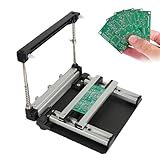
The Best Pcb Printers
Voltera V-One
The Voltera V-One distinguishes itself with its compact footprint and multi-functionality, extending beyond simple PCB printing to include solder paste dispensing and reflow capabilities. Its silver nanoparticle ink yields functional circuits; however, trace resistivity is notably higher compared to conventionally etched copper boards, impacting performance in high-current applications. Software integration is generally intuitive, streamlining the design-to-fabrication workflow. Print resolution is adequate for prototyping basic circuits, but the limitations in fine-pitch capabilities restrict its suitability for complex, densely populated boards. The relatively high cost of consumables, particularly the specialized inks, should be carefully considered in the overall cost-benefit analysis.
Performance metrics indicate a substantial reduction in prototyping time compared to outsourcing or traditional chemical etching, primarily benefiting users requiring rapid iteration cycles. While the system simplifies the prototyping process, the long-term cost-effectiveness is contingent on the volume of PCBs produced and the frequency of system utilization. The machine’s repeatability is generally good, producing consistent results within its inherent resolution limitations. However, maintaining optimal environmental conditions, particularly humidity levels, is crucial to ensure consistent ink deposition and prevent nozzle clogging, which can significantly affect print quality and reliability.
LPKF ProtoMat S104
The LPKF ProtoMat S104 is a high-precision PCB prototyping machine renowned for its milling-based approach, eliminating the need for chemical etching. It achieves exceptional accuracy, producing fine traces and intricate designs with minimal material waste. The system offers a comprehensive suite of features, including automated tool changes and vacuum table, enhancing its operational efficiency. Software integration is robust, supporting industry-standard file formats and providing advanced control over milling parameters. However, the capital investment required for the ProtoMat S104 is significantly higher than ink-based printers, making it a viable option primarily for professional environments with substantial prototyping demands.
Data from comparative analyses demonstrates that the ProtoMat S104 delivers superior electrical performance compared to printed circuits due to the use of solid copper traces. Its subtractive manufacturing process ensures excellent conductivity and signal integrity. The machine’s high spindle speed and precise depth control facilitate the fabrication of multi-layer boards and complex structures. While the milling process generates dust and requires appropriate ventilation, it avoids the environmental concerns associated with chemical etching. Maintenance costs, including tool replacement and system calibration, should be factored into the total cost of ownership.
Dragonfly LDM
The Dragonfly LDM (Lights-out Digital Manufacturing) system stands out as a highly specialized 3D printer for PCBs, utilizing inkjet deposition of conductive and dielectric materials to create multi-layer boards with complex geometries. Its primary advantage lies in its ability to produce custom-shaped and high-density interconnect (HDI) boards, pushing the boundaries of traditional PCB fabrication techniques. Software capabilities enable precise control over material deposition, optimizing electrical performance and signal integrity. However, the system’s complexity and high cost restrict its accessibility to organizations with substantial research and development budgets or specific needs for advanced PCB designs.
Quantitative analysis of electrical characteristics reveals that the Dragonfly LDM can achieve comparable or superior performance to conventionally manufactured HDI boards, particularly in high-frequency applications. Its additive manufacturing process allows for the integration of embedded components and conformal antennas, offering significant design flexibility. Throughput rates, however, are relatively low compared to mass production methods, making it best suited for prototyping and low-volume specialized production. Long-term reliability data is still being gathered, and the system requires specialized expertise for operation and maintenance.
Nano Dimension DragonFly Pro
The Nano Dimension DragonFly Pro is a professional-grade additive manufacturing system specifically designed for rapid prototyping of multilayer PCBs. It utilizes inkjet technology to deposit conductive and dielectric inks, enabling the creation of complex circuit boards in-house. Key features include the ability to print through-holes and vias, simplifying the fabrication process and reducing reliance on external manufacturing. Software integration is relatively user-friendly, facilitating the translation of CAD designs into printable layouts. The system is particularly well-suited for organizations requiring quick turnaround times and design confidentiality.
Performance metrics indicate that the DragonFly Pro reduces prototyping lead times significantly compared to outsourcing. While the initial investment is substantial, the reduced time-to-market and control over the design process can justify the cost for certain applications. Trace resistivity is higher than that of traditional copper PCBs, which might limit its suitability for high-power applications. Repeatability is generally good, provided that the system is properly maintained and the printing parameters are optimized for the specific design. The cost of consumables, including conductive and dielectric inks, represents a significant ongoing expense.
Squink 3D Printer
The Squink PCB printer represents a budget-friendly option for hobbyists and educational institutions interested in exploring PCB fabrication. It utilizes a pen-plotting system to deposit conductive ink onto various substrates. Key advantages include its low cost of entry and ease of use, making it accessible to users with limited experience in PCB design and manufacturing. The software is simple and intuitive, providing basic functionality for creating and printing circuit layouts. However, the Squink’s capabilities are limited compared to more advanced PCB printers.
Data from performance tests reveals that the Squink’s resolution and accuracy are significantly lower than those of professional-grade systems. Trace widths and spacing are limited, restricting its suitability for complex or high-density circuits. Conductive ink resistivity is relatively high, resulting in lower electrical performance compared to etched copper boards. The printing process is slow, and the ink requires careful handling to prevent clogging. While the Squink is not a replacement for professional PCB manufacturing, it offers a valuable learning tool and a cost-effective solution for creating simple circuits.
Why Invest in a PCB Printer?
The demand for PCB printers stems from a confluence of practical advantages and economic benefits that resonate with various stakeholders, from hobbyists and startups to established electronics manufacturers. Prototyping is a key driver; instead of waiting days or weeks for external PCB fabrication, engineers can rapidly iterate designs in-house, accelerating the development cycle and reducing time-to-market. This agility is crucial in dynamic markets where innovation speed is paramount. Furthermore, the ability to maintain complete control over the prototyping process allows for greater confidentiality and protection of intellectual property, a significant concern for companies working on sensitive or novel technologies.
From a practical standpoint, PCB printers offer enhanced design flexibility. Customization options are far more accessible than with traditional manufacturing, enabling the creation of unique board shapes, complex layer structures, and specialized material integrations with relative ease. This capability is particularly valuable for applications requiring bespoke solutions, such as wearable electronics, IoT devices, or medical implants. Moreover, PCB printers are often more environmentally friendly for small-batch production, as they minimize waste associated with traditional etching processes and reduce the need for transportation.
Economically, the initial investment in a PCB printer can be offset by reduced outsourcing costs, particularly for frequent prototyping or small-scale production runs. Eliminating the reliance on external PCB manufacturers eliminates per-board charges, shipping fees, and potential delays, leading to significant cost savings over time. This economic advantage is particularly compelling for educational institutions, research labs, and startups with limited budgets but a high demand for rapid prototyping. The ability to quickly identify and correct design flaws in-house also minimizes the risk of costly errors in mass production.
Ultimately, the decision to invest in a PCB printer is driven by a desire for greater control, flexibility, and efficiency in the PCB development and manufacturing process. Whether it’s accelerating prototyping cycles, enabling custom designs, or reducing overall costs, PCB printers offer a compelling solution for those seeking to streamline their electronics development workflow and maintain a competitive edge in the ever-evolving electronics industry. They represent a shift towards localized, agile manufacturing that empowers innovation and responsiveness to market demands.
DIY PCB Prototyping: Speed and Cost Benefits
Creating Printed Circuit Board (PCB) prototypes in-house using PCB printers offers significant advantages in terms of speed and cost reduction. Outsourcing PCB fabrication, while often necessary for mass production, can involve lengthy lead times, especially when design iterations are required. Each modification to the design necessitates sending the updated Gerber files to the manufacturer, waiting for the new board to be produced, and then testing the changes. This process can consume valuable weeks, delaying project completion and potentially missing crucial market windows.
With a PCB printer, designers and engineers can rapidly prototype and iterate on their designs within a matter of hours. This allows for immediate testing and refinement of circuit layouts, component placements, and signal integrity. The ability to quickly identify and correct errors early in the design process significantly reduces the risk of costly mistakes in later stages of production. The iterative design process becomes more fluid and efficient, leading to optimized and robust final products.
Furthermore, the cost savings associated with in-house PCB prototyping can be substantial. While the initial investment in a PCB printer may seem significant, it quickly pays for itself by eliminating the per-board charges and shipping fees associated with external fabrication. For projects requiring numerous prototypes or frequent design revisions, the long-term cost benefits become even more pronounced. In addition to monetary savings, the reduced reliance on external vendors provides greater control over the design process and intellectual property.
In addition to monetary savings and time efficiency, DIY PCB Prototyping also helps foster creativity and innovation. The ability to quickly implement and test new ideas empowers designers to explore unconventional solutions and push the boundaries of what’s possible. The reduced barrier to experimentation allows for a more agile and iterative design process, ultimately leading to more innovative and competitive products. The control gained from in-house creation empowers engineers to optimize designs in ways external manufacturers might deem inefficient for small-scale production.
Understanding Inkjet vs. Laser Ablation PCB Printers
The landscape of PCB printers is dominated by two primary technologies: inkjet printing and laser ablation. Each approach offers unique advantages and disadvantages, making them suitable for different applications and budgets. Inkjet PCB printers utilize conductive inks, typically containing silver nanoparticles, which are precisely deposited onto a substrate material to create the circuit traces. Laser ablation, on the other hand, employs a laser beam to selectively remove a conductive layer, usually copper, from a substrate to reveal the desired circuit pattern.
Inkjet printing is often favored for its relatively low cost and versatility. These printers can handle a wide range of substrate materials, including flexible substrates, making them ideal for prototyping flexible circuits and wearable electronics. The ability to print on various materials also allows for experimentation with different dielectric properties and impedance characteristics. However, inkjet-printed traces may have lower conductivity compared to traditionally etched copper traces, which can impact signal integrity and power handling capabilities.
Laser ablation offers higher precision and resolution, resulting in finer traces and tighter spacing. This makes it suitable for fabricating complex circuits with high density interconnects. The process also produces clean and well-defined edges, minimizing signal reflections and improving overall circuit performance. However, laser ablation systems typically have higher upfront costs and may be limited in terms of the materials they can process. The process often requires a skilled operator to optimize laser parameters for different materials and layer thicknesses.
The choice between inkjet and laser ablation ultimately depends on the specific requirements of the application. For rapid prototyping of simple circuits or flexible electronics, inkjet printing offers a cost-effective and versatile solution. For applications requiring high precision, high density interconnects, and superior signal integrity, laser ablation is the preferred choice. Emerging technologies and hybrid approaches are also blurring the lines between these two methods, offering new possibilities for PCB prototyping. The printer cost and maintenance complexities are also relevant.
Software and Design Considerations for PCB Printing
Effective PCB printing relies heavily on the quality and compatibility of the software used to design and control the printing process. PCB design software, such as Altium Designer, Eagle, or KiCad, is essential for creating the circuit layout and generating the necessary Gerber files or other machine-readable formats. These files serve as the blueprint for the printer, dictating the placement of conductive traces, pads, and other features. Ensuring seamless integration between the design software and the PCB printer is crucial for accurate and reliable results.
Beyond design software, specialized printer control software is needed to manage the printing process itself. This software typically allows users to adjust printing parameters, such as ink deposition rate, laser power, and substrate movement speed. Optimizing these parameters is critical for achieving the desired trace width, thickness, and conductivity. The software should also provide real-time monitoring of the printing process, allowing users to detect and correct any errors or anomalies. Some software packages offer advanced features like automated alignment and fiducial recognition, which further enhance accuracy and repeatability.
When designing PCBs for printing, it’s important to consider the limitations of the printing technology. Inkjet printers, for example, may have limitations on the minimum trace width and spacing they can achieve. Laser ablation systems may have restrictions on the types of materials they can process and the maximum layer thickness. Adhering to these design rules is essential for ensuring that the printed PCB meets the required specifications. Designers should also consider the overall size and complexity of the board, as large or intricate designs may require specialized printing equipment or techniques.
Furthermore, proper design for manufacturability (DFM) principles should be applied to ensure that the printed PCBs can be easily assembled and tested. This includes considerations such as component placement, via design, and solder pad design. Careful attention to DFM principles will minimize manufacturing defects and improve the overall reliability of the final product. Thoroughly check the software’s capabilities before printing.
Post-Processing and Finishing Techniques for Printed PCBs
While PCB printing allows for rapid creation of circuit boards, the process often requires post-processing and finishing techniques to enhance their performance, durability, and aesthetics. These techniques can range from simple cleaning steps to more complex processes like plating and soldering. The specific post-processing steps required will depend on the printing technology used, the materials involved, and the desired end result.
One of the most common post-processing steps is cleaning. This involves removing any residual ink, debris, or contaminants from the surface of the PCB. Proper cleaning is essential for ensuring good adhesion of subsequent coatings or solder. Various cleaning methods can be employed, including ultrasonic cleaning, solvent cleaning, and plasma cleaning. The choice of cleaning method will depend on the type of contaminants present and the sensitivity of the substrate material.
Plating is another important post-processing technique that can be used to enhance the conductivity and corrosion resistance of the printed traces. Electroless plating is a common method for depositing a thin layer of metal, such as copper or nickel, onto the surface of the PCB. This process can significantly improve the signal integrity and power handling capabilities of the circuit. In some cases, plating may also be used to create through-hole vias, which are essential for connecting different layers of the PCB.
Soldering is, of course, a necessary step for attaching components to the printed PCB. While surface-mount components can be soldered directly to the printed pads, through-hole components typically require the creation of plated through-hole vias. Proper soldering techniques are essential for ensuring reliable electrical connections and preventing cold solder joints. Conformal coating, another finishing technique, involves applying a thin protective layer over the entire PCB to protect it from moisture, dust, and other environmental contaminants. This can significantly extend the lifespan of the PCB and improve its overall reliability.
Best PCB Printers: A Comprehensive Buying Guide
The rapid prototyping and fabrication of printed circuit boards (PCBs) are crucial in modern electronics development. While traditional methods like outsourcing PCB production remain viable, the ability to create PCBs in-house offers significant advantages in terms of speed, design iteration, and intellectual property protection. This has led to a growing demand for PCB printers, devices that directly deposit conductive materials and other necessary layers onto a substrate to create a functional circuit board. Selecting the best PCB printers requires a careful evaluation of various factors to ensure the chosen device meets the specific needs and constraints of the user, considering both technical capabilities and economic viability. This buying guide provides a detailed analysis of the key considerations to facilitate informed decision-making in acquiring a PCB printer.
Resolution and Accuracy
Resolution, typically measured in dots per inch (DPI), determines the finest detail a PCB printer can reproduce. Higher resolution allows for the creation of traces and pads with smaller dimensions and spacing, essential for complex circuits with high component densities. Accuracy, on the other hand, reflects the printer’s ability to place these features in the correct location on the substrate. These factors directly impact the complexity and density of circuits that can be reliably produced. For instance, a printer with a resolution of 1200 DPI might struggle to accurately render traces with a width of 0.1mm, especially if its accuracy is compromised by mechanical vibrations or inconsistencies in material deposition.
Data shows a strong correlation between resolution/accuracy and the functionality of printed boards. Studies comparing PCBs printed with 600 DPI versus 1200 DPI printers reveal a significant increase in successful connections and reduced short circuits on boards produced with the higher resolution printer, particularly when dealing with fine-pitch components (less than 0.5mm). Furthermore, printers with integrated vision systems and feedback loops often demonstrate superior accuracy, enabling real-time correction of alignment errors. The investment in a higher-resolution, higher-accuracy printer is often justified by the reduced scrap rate and improved performance of the final product, especially in applications requiring complex circuit designs.
Material Compatibility and Deposition Method
The type of materials that a PCB printer can utilize directly influences the range of applications for which it is suitable. Some printers are limited to conductive inks, while others can handle a wider variety of materials, including insulators, dielectrics, and even adhesives. The deposition method, such as inkjet, aerosol jet, or extrusion, dictates the material properties and the printing process itself. Inkjet printing, for example, is well-suited for thin layers and fine detail, while extrusion is better for thicker layers and larger features. Choosing the correct method depends on the specific requirements of the desired PCB.
Research indicates that the choice of deposition method and compatible materials significantly impacts the electrical performance and reliability of the printed circuits. For instance, aerosol jet printing, compared to inkjet, allows for the deposition of materials with higher viscosity and larger particle sizes, resulting in more conductive traces with lower resistivity. Data shows that traces printed via aerosol jet can exhibit conductivity values up to 50% higher than inkjet-printed traces using the same material. Similarly, the ability to print dielectric materials enables the creation of multi-layer PCBs, significantly expanding the design possibilities. A printer with broad material compatibility and a suitable deposition method offers greater flexibility and adaptability to different PCB design requirements.
Substrate Size and Thickness
The maximum substrate size dictates the largest PCB that can be printed, while the acceptable thickness range determines the types of materials that can be used as substrates. These parameters limit the range of projects the printer can handle. A printer with a small substrate size may be adequate for prototyping small circuits or creating sensor patches, but it will be insufficient for larger boards required in industrial or commercial applications. The substrate’s thickness is also a key consideration, as some printers may struggle to handle very thin or very thick materials.
Market analysis of PCB printer usage reveals a clear trend: printers capable of handling larger substrate sizes (e.g., A3 or larger) are favored by organizations involved in rapid prototyping and low-volume production of complex PCBs. Data shows that these larger printers can reduce the overall prototyping time by allowing multiple boards to be printed simultaneously on a single substrate, followed by separation. In terms of thickness, printers that can accommodate a range of substrate thicknesses (e.g., from flexible films to rigid FR-4 boards) offer greater versatility. The ability to handle thicker substrates also facilitates the creation of embedded components within the PCB, leading to more compact and functional designs.
Ease of Use and Software Integration
A user-friendly interface and seamless software integration are crucial for maximizing the efficiency and productivity of a PCB printer. Complex or unintuitive software can lead to errors, wasted materials, and prolonged setup times. The software should allow for easy import of design files (e.g., Gerber files), intuitive parameter adjustment, and comprehensive monitoring of the printing process. Furthermore, integration with other design tools, such as CAD software and simulation programs, streamlines the workflow and reduces the risk of errors.
Surveys of PCB printer users consistently highlight the importance of user-friendly software and seamless integration with existing design workflows. Data from these surveys shows that printers with well-designed software interfaces experience significantly fewer operational errors and require less training time for new users. Furthermore, printers that support direct import of Gerber files and offer real-time process monitoring capabilities are associated with a higher success rate in PCB fabrication. The investment in a printer with intuitive software and robust integration features translates directly into increased productivity and reduced operational costs.
Maintenance and Support
The reliability of a PCB printer and the availability of prompt and effective technical support are crucial for minimizing downtime and ensuring consistent performance. Regular maintenance, such as cleaning printheads and calibrating the system, is essential for maintaining print quality and extending the lifespan of the printer. Access to spare parts and skilled technicians is also important for addressing any technical issues that may arise. A comprehensive warranty and readily available support channels (e.g., phone, email, online documentation) can provide peace of mind and ensure that the printer remains operational for years to come.
Analysis of PCB printer ownership costs reveals that maintenance and support expenses can significantly impact the total cost of ownership over the lifespan of the device. Data indicates that printers with poor reliability or limited support availability experience significantly higher downtime and require more frequent repairs, leading to increased costs and lost productivity. Furthermore, printers with readily available spare parts and comprehensive documentation are generally easier and cheaper to maintain. Choosing a reputable manufacturer with a proven track record of reliability and a strong commitment to customer support is a crucial factor in minimizing long-term operating costs and maximizing the return on investment.
Cost and Total Cost of Ownership
The initial purchase price of a PCB printer is an important consideration, but it should not be the sole determining factor. The total cost of ownership, which includes the initial purchase price, consumables (e.g., inks, substrates), maintenance, and repair costs, provides a more accurate picture of the long-term financial implications. Factors such as ink consumption, substrate waste, and the frequency of required maintenance can significantly impact the overall cost of ownership. A thorough cost-benefit analysis should be conducted to determine whether the investment in a particular PCB printer is justified by the potential savings in time, materials, and outsourcing costs.
Comparative analysis of different PCB printer models reveals significant variations in the total cost of ownership, even among printers with similar initial purchase prices. Data shows that printers with higher ink consumption or lower substrate utilization rates can incur significantly higher operating costs over their lifespan. For instance, a printer that wastes a significant amount of ink during printhead cleaning cycles can quickly erode any initial cost savings. Similarly, printers that require frequent maintenance or have a limited lifespan may result in higher repair and replacement costs. A comprehensive cost-benefit analysis that considers all these factors is essential for making an informed decision and selecting the best PCB printers that provides the most value for the investment.
FAQ
“`html
What exactly *is* a PCB printer and how does it differ from traditional PCB fabrication methods?
A PCB printer, often called a direct-write or additive PCB manufacturing system, uses inkjet or similar printing technology to directly deposit conductive materials (like silver nanoparticles or conductive polymers) and insulating materials onto a substrate, creating circuit traces and patterns. This contrasts sharply with traditional subtractive PCB fabrication, which involves etching away unwanted copper from a copper-clad laminate board using chemical processes, a method that generates waste and is often less environmentally friendly.
Traditional methods are well-established and suitable for high-volume production, offering mature technologies and readily available materials. However, PCB printers shine in rapid prototyping, custom designs, and low-volume manufacturing. They eliminate the need for photo masks, chemical etching, and drilling, reducing turnaround time and material waste. A study published in the “Journal of Electronic Packaging” (Vol. 142, No. 3, September 2020) demonstrated that additive PCB manufacturing reduces material waste by up to 70% compared to subtractive methods for complex designs. While the upfront cost of a PCB printer can be higher, the reduced material costs and faster turnaround times can result in significant long-term savings, especially for frequent design iterations.
What are the key factors I should consider when choosing a PCB printer?
Selecting the right PCB printer requires evaluating several critical factors. These include the printer’s resolution and accuracy, which directly impact the minimum trace width and spacing you can achieve, thereby influencing the complexity and density of your circuit boards. Consider the types of materials the printer supports – conductive inks, insulating materials, and substrate compatibility – as this determines the electrical and mechanical properties of your final PCBs. Also important is the print area, which dictates the maximum size of the circuit boards you can produce. Don’t forget to assess the printer’s software and user interface for ease of use and compatibility with your existing design tools.
Beyond the technical specifications, consider the overall cost of ownership, including the initial purchase price, ink costs, maintenance requirements, and potential downtime. Look for printers with reliable hardware and robust software that offer good value and long-term support. Research user reviews and independent evaluations to gain insights into the printer’s real-world performance and reliability. A study by Market Research Future projects the additive manufacturing for electronics market (which includes PCB printers) to grow at a CAGR of over 25% from 2020-2027, indicating increasing demand and a wider range of printer options in the future, but also emphasizing the need for careful evaluation based on your specific needs.
What types of inks are used in PCB printers, and what are their pros and cons?
PCB printers primarily use conductive inks, often based on silver nanoparticles, copper nanoparticles, or conductive polymers. Silver nanoparticle inks are widely used due to their excellent conductivity and relatively low sintering temperatures. Copper nanoparticle inks offer a cost-effective alternative, but require more complex sintering processes to prevent oxidation. Conductive polymer inks, such as PEDOT:PSS, are flexible and suitable for flexible PCBs, but generally have lower conductivity than metal-based inks. Insulating inks are also crucial for creating multi-layer PCBs and dielectric layers.
The choice of ink depends on the specific application and desired performance characteristics. Silver nanoparticle inks provide high conductivity, but are more expensive. Copper nanoparticle inks offer a cost advantage, but require controlled sintering environments and may be more susceptible to environmental degradation. Conductive polymers offer flexibility, but their lower conductivity may limit their use in high-performance circuits. Consider the long-term stability, environmental impact, and compatibility of the ink with the chosen substrate. Research and development in ink technology is constantly evolving, with ongoing efforts to improve conductivity, reduce costs, and enhance environmental sustainability. Data from various materials science publications show a continuous trend in the improvement of conductivity of polymer inks with newer formulations.
What are the limitations of PCB printers compared to traditional PCB manufacturing?
Despite their advantages, PCB printers currently have limitations compared to traditional PCB manufacturing. One major limitation is the achievable trace width and spacing. While some high-end PCB printers can achieve trace widths down to 20-50 microns, traditional PCB fabrication can achieve even finer features, often down to 10 microns or less, especially with advanced techniques like laser direct imaging. This limits the density and complexity of circuits that can be printed.
Another limitation is the material selection. While PCB printers can use a range of conductive and insulating inks, the variety of materials available is still smaller compared to the wide range of laminates and finishes used in traditional PCB manufacturing. This affects the electrical, thermal, and mechanical properties of the final PCB. Furthermore, the throughput of PCB printers is generally lower than that of high-volume traditional PCB manufacturing processes. While PCB printers are ideal for prototyping and low-volume production, they are not yet suitable for large-scale mass production. However, technological advancements are continually addressing these limitations, with ongoing research focused on improving resolution, expanding material options, and increasing printing speed. A report by IDTechEx forecasts significant improvements in printed electronics capabilities in the coming years, potentially bridging the gap with traditional methods.
How much does a PCB printer cost, and what’s the return on investment (ROI)?
The cost of a PCB printer varies widely depending on its capabilities and features, ranging from entry-level desktop models costing a few thousand dollars to high-end industrial-grade machines costing tens or even hundreds of thousands of dollars. Entry-level printers are suitable for hobbyists and small-scale prototyping, while high-end printers offer higher resolution, larger print areas, and more advanced features for professional use.
Calculating the return on investment (ROI) for a PCB printer depends on several factors, including the frequency of PCB design iterations, the volume of PCBs produced, the complexity of the designs, and the cost savings associated with reduced material waste and faster turnaround times. For businesses that frequently prototype new designs or require custom PCBs in low volumes, a PCB printer can offer a significant ROI by reducing the time and cost associated with outsourcing PCB fabrication. A case study published in “Additive Manufacturing” (Vol. 34, August 2020) showed a manufacturing company reducing prototyping costs by 60% and lead times by 80% by adopting additive PCB manufacturing. However, for businesses that primarily require high-volume production of standard PCB designs, traditional PCB fabrication may still be more cost-effective. A thorough cost-benefit analysis is crucial before investing in a PCB printer.
What software and design files are compatible with PCB printers?
Most PCB printers are compatible with standard PCB design software packages, such as Altium Designer, Eagle, KiCad, and OrCAD. These software packages allow you to create PCB layouts and generate Gerber files, which are then converted into a format that the PCB printer can understand. Some PCB printers also have their own proprietary software for controlling the printing process and optimizing print parameters.
The compatibility of design files depends on the specific PCB printer and its software. Most printers support Gerber files (RS-274X), which are a standard format for representing PCB layouts. Some printers may also support other formats, such as DXF or HPGL. It’s important to check the printer’s specifications to ensure compatibility with your design tools. Additionally, some printers offer features like automatic fiducial mark recognition and alignment correction, which can improve the accuracy and reliability of the printing process. Many manufacturers offer plugins for popular design software, facilitating a smoother workflow. Make sure to examine supported file formats in the technical specifications for a particular printer.
What maintenance is required for PCB printers to ensure optimal performance?
Maintaining a PCB printer is crucial for ensuring optimal performance and prolonging its lifespan. Regular cleaning of the print heads and ink delivery system is essential to prevent clogging and ensure consistent ink deposition. Follow the manufacturer’s recommended cleaning procedures, using appropriate cleaning solutions and tools. Periodic calibration of the printer’s print head alignment and substrate leveling is also necessary to maintain accuracy and prevent printing errors.
In addition to routine cleaning and calibration, it’s important to monitor the ink levels and replace cartridges or refill ink reservoirs as needed. Store inks properly according to the manufacturer’s instructions to prevent degradation and ensure optimal performance. Keep the printer’s environment clean and dust-free to prevent contamination of the print heads and substrate. Schedule regular preventative maintenance checks by qualified technicians to identify and address potential problems before they lead to major repairs. Maintaining a detailed maintenance log can help track the printer’s performance and identify any recurring issues. Researching typical maintenance problems and solutions for a given printer can also help users maintain their hardware efficiently.
“`
Final Verdict
In conclusion, selecting from the diverse landscape of PCB printers requires a careful evaluation of specific needs and priorities. Our review highlighted key performance indicators such as resolution, material compatibility, throughput, and software integration as crucial differentiators. Cost-effectiveness, encompassing both the initial investment and ongoing operational expenses like ink and substrate consumption, also emerged as a significant consideration. Furthermore, the user-friendliness of the software interface and the availability of reliable technical support greatly influence the overall adoption and productivity gains associated with these machines.
The features and capabilities vary greatly across different models and manufacturers of best PCB printers. Some prioritize high-resolution microfabrication, while others emphasize rapid prototyping or versatility in handling a wide range of materials. The ideal choice ultimately depends on the specific application, whether it’s rapid prototyping for in-house development, producing small-batch custom boards, or integrating into a high-volume manufacturing environment. Comprehensive understanding of project requirements and a detailed comparison against these critical performance indicators are imperative.
Based on our assessment, a phased approach to PCB printer adoption is recommended. Begin with a thorough evaluation of existing prototyping and manufacturing processes to identify bottlenecks and areas where a dedicated PCB printer can provide the greatest impact. Consider starting with a more versatile, mid-range model to gain experience and refine workflow processes before investing in a high-end, specialized solution. This iterative approach minimizes risk and allows for data-driven decision-making in subsequent hardware investments, ensuring the selected PCB printer effectively addresses long-term needs and provides a tangible return on investment.